RESOURCES
Every printed circuit board (PCB) should be able to operate without disruption due to interference from other devices and without causing interference. To accomplish this, PCBs need to have strong electromagnetic compatibility (EMC) built-in from the ground up.
EMC is what keeps our devices from constantly interfering with each other. The high amount of wireless devices in use today — phones, radios, computers, remotes — are all becoming more complex and more interconnected. In the past, when such devices were less common, and interference was low, a car radio could be enough to disrupt a TV set. Now, EMC is more of an area of focus, and every PCB is expected to use these design practices to minimize unwanted emissions. With proper design, you can pass EMC compliance testing the first time.
This design concept is much easier to implement from the start. Often, designers leave EMC untouched until the testing phase. Adding EMC in after the board has already been developed can cost significant time and money
Design for EMC Compliance
Designing electronic systems for EMC can help you stay one step ahead by minimizing problems in the first place. Below are some EMC design techniques that you can implement to pass electromagnetic compatibility testing.
1. Board Layout
It is important to consider the signals that will be given off by your board. Some of these will be intentional, but 90% of electromagnetic interference (EMI) emissions from a PC board will be unintentional. Some of these unintentional signals are from common-mode currents, crosstalk coupling to I/O traces and power planes.
Radiated emissions (RE) can come from a variety of sources in your PCB, but one common area is cables, which can be tricky to minimize because of the high-frequency signals and data they may need to carry.
One approach is to filter the cables as they enter and leave the unit, but you'll want to be careful about this. While a filter does reduce the EMI levels, it can also degrade the circuit functioning. In a high-speed data circuit, the filter will remove any sharp edges and may degrade the signal to the point where it doesn't work. At this point, you'll need to balance your performance needs with EMI reduction.
When drawing out your traces, you will want to minimize the loop areas for high-frequency signal and power currents. High-frequency signal currents return to their source, meaning they are always loops. They also take the path of least impedance, which tends to be the path with the smallest loop area. A current will return as close as possible to the outgoing current's path.
Lower frequencies look for the path of least resistance. They can be harder to find because they spread out more. Outgoing and return paths may be distant from each other in this case.
A few more general principles for controlling radiated emissions by design include the following.
- Increase trace width where possible. A wider trace size is shown to effectively decrease radiated emissions.
- One way to shield your inner layers from radiation is by filling your top and bottom layers with a solid ground plane and using ground-stitch vias throughout the PCB. Metalizing your PCB edges with copper plating may also help to decrease radiation from the inner layers and increase the cooling efficiency.
- Add stitching vias between your layers and near high-speed signal vias to keep current loops as small as possible.
- Avoid 90-degree angles if working with very high-speed applications.
2. Filters
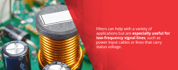
Filters can help with a variety of applications but are especially useful for low-frequency signal lines, such as power input cables or lines that carry status voltage. In these instances, EMI filters can remove the high-frequency elements, leaving only low frequency on the line that generates much less radiation.
These filters should be used at the entry point between the equipment and its environment, bonded tightly to the chassis. This placement ensures that no signals enter the unit and radiate it before being removed by the filter. They can also be placed in between segregated areas of your PCB or between the boards of a module.
Several different filters can be used for various purposes in your PCB. Of these, two main types focus on absorption and reflection. In an absorption filter, unwanted energy is absorbed by the filter. This type is preferred for EMC applications. In a reflective filter, the unwanted signal bounces back to the line. An EMC filter placed at the edges of your unit can help reduce EMC issues.
The low-pass filter retains the low-frequency signals and rejects high-frequency ones. This is the most common type of filter, but bandpass filters can also be used and will accomplish the same goal.
Filters come in several formats, such as a resistor or ferrite placed around a wire or cable. For more advanced uses, they might need to be made up of several components. Astrodyne TDI has a wide catalog of filters, and if you need something more specific, our team of engineers can find you an EMI solution that fits your equipment at industry standards.
You may also want to consider decoupling. Decoupling capacitors stabilize the voltage coming into the device and decrease electrostatic discharge (ESD), which we will talk about in more detail in the next section.
3. Circuit Partitioning
This part of your PCB design is essential to do correctly from the start, as it determines the entire map of your circuit board. Not only does it organize your board, but it also optimizes the placement of high- and low-noise circuitry so that they don't interfere with each other.
Partitioning your circuit allows you to separate the circuit into EMC critical and non-critical areas. Critical areas are those that contain sources of radiation or may be susceptible to it, including high-frequency circuits, low-level analog circuits and high-speed microprocessor circuits. Non-critical areas include circuitry that is unlikely to radiate signals or be vulnerable to them, including slow-speed circuits and linear power supplies.
By partitioning your circuit, you can add screens or filters to isolate these areas from the effects of EMI. It helps to make the lines as short as possible. You'll also want to keep noisy or high-speed lines away from the edge of the board and place non-noisy traces away from high-noise areas, such as by connectors and oscillator circuits. Doing this keeps the voltage differences between the connectors to a minimum, preventing the current from reaching attached cables and creating EMC problems.

4. Grounding
Poor grounding can be bad news for your EMC performance. It can lead to ground loops, resulting in radiated emissions or signals picked up from within the unit. Remember that a grounding system creates a path to return a current to its source. It needs to have low impedance and be as direct as possible.
- One way to help this process is to place a ground plane directly below the plane with your signal traces. This plane can shield against EMI. It offers low inductance and low resistance common ground, creating a short lead length to the ground. For some areas, you may need to isolate the ground so ground currents can't flow across the section.
- Never route signals over a split ground plane. Doing this can create large loops and high radiated emissions since the return current can't flow under or beside the forward current.
- The length of a grounding system should be kept to a minimum, to prevent inductance from becoming a problem. At low frequencies, this impact can become quite significant. Thick wires can help, as well as using ground planes with critical tracks on your PCB.
- Gridding is another method you can use to improve EMC performance in a board with few layers. Gridding expands any ground traces and fills up as much empty space on the PCB as possible. This process generates a network of connections between the traces that are carrying ground. It works similarly to a ground plane and provides a ground return path under each signal trace, lowering the impedance between the main ICs and the voltage regulation area.
- Use shielded or twisted cables. These can both protect your cables from released emissions and prevent them from releasing their own emissions.
- Connect your ground plane to the chassis where the cable leaves and enters the chassis so they have the same potential at the IO area.
5. Shielding Lines, Cables and Enclosures
There are several different ways to protect an optimized PCB from further EMI through shields. A shield is a type of barrier that can be used in conjunction with other noise-suppression methods such as grounding and filtering. The effectiveness can vary based on the material's conductivity and thickness, among other factors. Heating is also an aspect of this, as some enclosures will have apertures in the structure to allow airflow without sacrificing EMC.
You can use an enclosure, along with gaskets and filters, to try and cover as much of the unit as possible. You want to "seal" up the board from as much outside emission as possible. A unit placed in an enclosure can see great improvements to its EMC performance, not to mention it gives it some structural strength.
Shields can be used on incoming cables to protect against unwanted signal radiation or external signals. Most shielded cables will have an insulation layer and braided conductors. These may not be as effective at a low frequency and become stronger at higher frequencies.
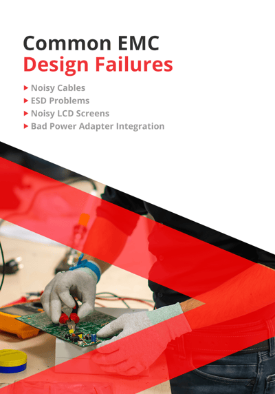
Common EMC Design Failures and How to Avoid Them
While designing for EMC can alleviate most problems and ensure that you meet the Federal Communications Commission's EMC design requirements, there are a few common problems that people tend to encounter when dealing with EMC issues. Most of these problems come down to radiated emissions (RE).
1. Noisy Cables
Cables work like antennas by attracting and even amplifying noise. You'll need to keep these characteristics in mind and be careful about how you implement your cables so you can reduce EMI as much as possible. You'll need to minimize the unintentional noise that is coupled with both external and internal cabling.
- One aspect you'll want to keep in mind is the slew rate. The slew rate measures how much the voltage or current changes over time. Higher slew rates occur when the signal contains more energy at a higher frequency. This high level of energy can be a source of heavy radiation. By using a low-pass filter or reducing the driver strength, you can usually reduce the slew rate.
- Keep signal lines clear. DC signals from power supplies and IO signals can bring RF energy to your cables. Some of these can grab heavy amounts of RF noise as they travel through your board, then release it as radiation.
- Add ferrite beads to reduce noise. These can suppress the noise coming off of your cables, and if you're using bypass capacitors, you may even end up with an LC (inductor-capacitor) filter.
- Decouple power supply connectors. Decoupling capacitors should be as close as possible to the power pin on the device. These capacitors minimize the loop current of a power supply.
2. ESD Problems
Your PCB will usually undergo electrostatic discharge (ESD) testing. ESD can cause a high number of failures in your device, such as a reset or damage to some parts.
In a board with a non-conductive chassis, there likely won't be too many discharge points, but there are still some common problem areas, including connectors, buttons, screw heads and LEDs or graphic displays.
Including an ESD suppressor close to where the discharge is likely to occur can keep your voltage to a manageable level by dissipating extra energy as heat or noise.
3. Noisy LCD Screens
An LCD display can heavily influence your device's EMI. Individual screens vary widely across manufacturers in terms of how high their radiated emissions are. You may need to try several to find one that offers low emissions rates.
4. Bad Power Adapter Integration
A power adapter can have a significant influence on the noise levels of your device and its EMC. Different products have different classes, and you'll need to select the right one for your device. Class A is for devices exclusive to business, commercial and industrial environments, while Class B can be used anywhere. Class B devices have stricter testing than Class A ones, so using the correct power supply is important. There are also different standards for medical and military environments.
You'll still need to minimize the RF current demands on your power adapter and ensure that the specifics of your device keep emissions levels low.

Implement EMC and EMI Design Guidelines Today
Many factors go into designing a PCB, but EMC design considerations are some of the most foundational. Ensuring that you minimize your EMI will help you design for EMC compliance standards.
By considering EMC design guidelines in your PCB grounding techniques, connector selections, filters and circuit partitioning, among other features, you can choose the most effective materials and design methods for your product and pass compliance testing the first time.
Astrodyne TDI offers a variety of EMI filters and power supplies to help you reach your PCB design goals. If you have any questions about how you can use these products to optimize your PCB for EMI and EMC testing, contact us today.