RESOURCES
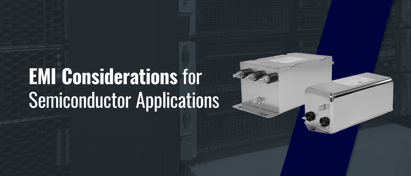 Practically every electronic device is susceptible to electromagnetic interference (EMI). Coming from both natural and engineered sources, EMI presents equipment risks, especially in semiconductor manufacturing. Manufacturers need to recognize and defend against causes of EMI. Here, we will discuss some of the primary causes of EMI, its effects on semiconductor manufacturing and how EMI filters can help.
Common Causes of EMI
Electromagnetic interference is broadly defined as an electrical or magnetic emission that negatively affects the functionality of electronic equipment. Everything that uses electricity can generate emissions that can turn into EMI. The sources of emissions typically fall into one of two categories:
- Narrowband emissions: Narrowband emissions are artificial emissions that are typically limited to a small area of the radio spectrum and may be continuous or sporadic. For example, power lines and brush motors produce a continuous low level of narrowband emissions.
- Broadband emissions: Broadband emissions affect a larger area of the electromagnetic spectrum. These can be continuous or sporadic and may be natural or human-made in origin. Some common examples include lightning strikes and arc welders.
Emissions can be generated inside electronic devices by impedance, opposition to current, voltage variances, and interconnecting wiring. Outside of a device, solar flares, telephone lines, nearby appliances, and power lines can also generate emissions. These emissions may not be damaging in nature, but once they start to cause problems, they become EMI.
EMI can effectively disrupt devices and systems, sometimes in critical systems such as medical and aerospace electronics. While emissions may only cause temporary disturbances, some EMI may cause catastrophic data losses and system failures. As a result, engineers in facilities that utilize sensitive equipment need to assess and protect against EMI risks.
Semiconductor Functions and Applications
A semiconductor, at its most basic, is a substance with the properties of both a conductor and an insulator. The properties of semiconductors make them a good medium for controlling the flow of electricity, turning it on and off as needed. They can handle a range of currents and voltages, and they can be integrated into microelectronic circuits. Due to their compactness, reliability, efficiency, and relatively low cost, semiconductors are gaining increasing popularity across various applications. Semiconductors are commonly used in a range of electronic and power devices, including diodes, transistors, integrated circuits, and solid-state lasers.
In the future, semiconductors are expected to grow in usage throughout consumer and industrial applications. The global sale of semiconductors exceeded $466 billion in 2020 and that number is expected to increase in the coming years. As a result, semiconductor manufacturing is expected to expand considerably with rising demand.
The Semiconductor Manufacturing Process
Semiconductors are produced in a highly controlled environment using specialized equipment. The process is split into two phases — "front-end," which covers wafer processing, and "back-end," which covers testing, assembly and packaging:
- Front-end processes: Front-end semiconductor manufacturing processes include wafer production, epitaxy, photolithography, oxidation, etching, stripping, deposition and chemical mechanical planarization. Each process involves adding or etching away at layers on the surface of the to-be semiconductor. Various inspections are performed at each stage to monitor the product and process and to maintain quality. Overall, these processes are performed in a series of 16 to 24 loops.
- Back-end processes: Back-end semiconductor manufacturing processes include testing, assembly and packaging. During this phase, finished wafers are tested, split into individual chips, then packaged for shipment.
While these descriptions are not exhaustive, they touch on the amount of equipment and processing involved in the semiconductor manufacturing process. At any stage, EMI can present a danger to the final product.
Identifying EMI in Semiconductor Applications
Electromagnetic environments in today’s semiconductor manufacturing facilities present some significant challenges. Semiconductor equipment has become increasingly sensitive to EMI as equipment has decreased in size. This means that even small emissions can cause errors and downtime. This can result in the following problems for manufacturers:
- Process errors: Strong EMI can result in software errors, parametric errors, and malfunctions, which may alter the process enough to produce a faulty product.
- Equipment downtime: Some tools may be strongly affected by EMI to the point where they may lock up or malfunction. At this point, the tool can no longer produce the required yield, resulting in costly downtime.
- Faulty tests: False positives and false negatives in sensors and tests can be extremely costly. Faulty sensors can often halt the manufacturing process with a faulty product. In worst-case scenarios, these faulty tests can result in a malfunctioning product being shipped to a customer.
- Device damage: Strong EMI can also damage sensitive devices and components. This is especially true in processes that involve metal-to-metal contact.
All these problems can result in significant costs to semiconductor manufacturers.
Reducing EMI in Semiconductor Manufacturing Environments
Managing the electromagnetic environment in semiconductor manufacturing environments is a complex task. Minimizing EMI in the semiconductor manufacturing process requires understanding the types and causes of EMI common to the environment and introducing management solutions.
Types of EMI
Though EMI is common in semiconductor manufacturing environments, the nature of EMI varies widely. Some key characteristics of EMI to consider in these environments include:
- Radiated and conducted emissions: Radiated emissions are emissions that escape equipment in the form of electromagnetic fields, while conducted emissions are carried out of equipment through attached cables.
- Far fields and near fields: Near and far-fields are critical considerations for EMI. Near fields are defined as distances from a source that are less than the wavelength of the emission, while far fields are distanced greater than the wavelength. Near and far-fields are critical to know for EMI testing, as they determine how far EMI travels from a source.
- Continuous and transient signals: EMI is further described as either continuous or transient. Continuous EMI is usually low-voltage, consistent, and is generally produced by lighting, power sources, and electric brush motors. Transient EMI is short-term and can be high or low-voltage. Lightning and arc welder surges are common examples of this.
Knowing the various types and characteristics of EMI within semiconductor manufacturing environments is the first step to understanding how to manage EMI effectively.
Causes of EMI
Once you understand the different types and characteristics of EMI, the next step is to understand EMI causes. EMI is commonly generated in semiconductor environments in three ways:
- ESD events: Also known as discharges, ESD events are rapid drops in static voltage followed by a surge of discharge current. The electromagnetic field formed as a result is transient, but it can have a significant effect on surrounding equipment depending on the discharge voltage.
- Parasitic emissions: Parasitic emissions are unintentional electromagnetic emissions produced by the equipment. These emissions are often a result of improper connections or configurations. When the equipment is on, electromagnetic emissions generated by the equipment leak out and potentially affect surrounding equipment. The nature of this EMI varies based on the type of equipment it comes from.
- Intentional radiation: Some equipment generates EMI as part of normal operation even when it is configured correctly. When placed too close to sensitive equipment, this EMI-generating equipment can disrupt normal operations.
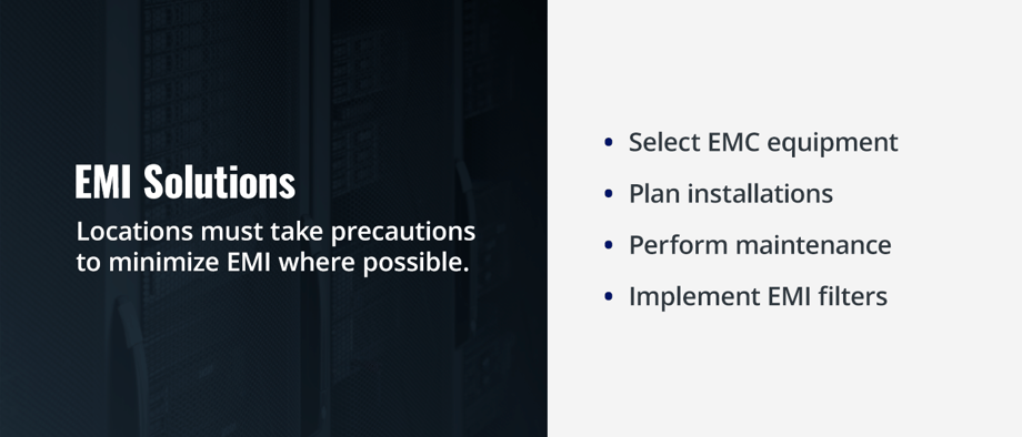
EMI Solutions
To prevent EMI in semiconductor manufacturing industry facilities, locations must take precautions to minimize EMI where possible. This includes implementing EMI best practices, including:
- Select EMC equipment: Semiconductor fabrication is becoming an increasingly sensitive process, so it is critical for manufacturers to take EMC compliance (EMC) into consideration. Only buy equipment that meets appropriate EMC standards.
- Plan installations: Manufacturers must also pay close attention to the placement of their equipment. Equipment that produces intentional radiation must be placed away from sensitive equipment. Similarly, equipment that is prone to producing parasitic or conducted emissions should not be placed on the same ground or power lines as more sensitive pieces.
- Perform maintenance: Perform maintenance regularly to ensure optimal equipment functionality. Make sure maintenance tools are not left with disconnected grounds or open covers, as these can result in EMI.
- Implement EMI filters: Protect equipment from interference by installing EMI suppression filters where conducted emissions pose a risk. These filters can help reduce or eliminate this type of interference.
EMI Compliance Regulations for Semiconductor Applications
When considering EMI solutions for semiconductor applications, compliance regulations should also be taken into account. The SEMI standards organization provides a range of regulation materials addressing the unique challenges of the semiconductor manufacturing industry. SEMI 176-1017, “Guide to Assess and Minimize Electromagnetic Interference (EMI) in a Semiconductor Manufacturing Environment” was published in 2017 to specifically address managing EMI in a semiconductor fab environment. It is a valuable resource for learning more about EMI and management solutions.
SEMI E176-1017 covers the following topics:
- Fundamentals: This section is a primer that explains the types of EMI in semiconductor environments, outlines properties of EMI that are harmful, and covers the effects of EMI on equipment and semiconductor devices.
- Measurements: This section highlights the importance of measurement for assessing EMI in semiconductor environments. It explains how to take measurements properly, and it also outlines the types of measurements to take and the distances at which to take them. This section emphasizes the importance of taking measurements according to the practical use and operability of equipment, rather than EMC regulation standards.
- EMI audits: EMI surveys and audits are essential for EMI control in factory settings. These audits map EMI levels in facilities, verify compliance with internal and external EMI limits, identify sources of emission and pinpoint potential improvements. This section of SEMI E176-1017 outlines the parameters of these audits and highlights the importance of performing regular EMI audits as proactive measures against damaging EMI.
- Mitigation: This section is the core part of the document and outlines practical guidance on how to contain and control EMI. Practical measures such as proper coverings and fixtures are a big part of this section, but it also addresses the importance of utilizing EMI filters.
- Recommended EMI limits: The final section of the document covers recommended EMI limits in the far and near field.
Implementing SEMI E176 principles is one of the best ways to manage EMI in semiconductor environments. One way to get started is by selecting and installing quality EMI filters.
Using EMI Filters in Semiconductor Applications
EMI filters are powerful tools across electronics applications for minimizing electromagnetic interference. EMI filters work by using two types of components to suppress conducted electromagnetic signals:
- Capacitors: Capacitors in EMI filters are called shunting capacitors. In general, capacitors inhibit direct currents while allowing alternating currents to pass through. Shunting capacitors redirect current within a specific range away from the circuit or component they are attached to.
- Inductors: Inductors are small electromagnets that hold energy as electric currents pass through, reducing the total voltage. When a capacitor redirects a current away from a component, the inductors reduce the voltage of this current as it passes through them.
When used in practice, EMI filters are applied to equipment to suppress electromagnetic noise transmitted through conduction. In use, they redirect and reduce currents flowing toward sensitive equipment, shorting the current to the ground. EMI filters are commonly used on a range of sensitive equipment, such as laboratory and medical equipment. However, their use can also benefit semiconductor manufacturing by helping protect sensitive equipment from conducted EMI in the environment.
EMI Filters and Considerations
If you are using an EMI filter, it is critical to choose the right filter for your application. Device designers should consider the following characteristics of EMI filters when making their selection:
- Filtering properties: EMI filters have varying filtering properties to handle different types of signals. The most common type is a low-pass EMI filter, which allows low-frequency signals to pass through while blocking higher frequency noise. To assess a filter for an application, analyze its filtering properties. Insertion loss values express the ratio of strength between an incoming signal and its transmitted signal frequencies of interest. The equivalent series resistance (ESR), Q factor, and dissipation factor (DF) are also good values to analyze that indicate the quality of the filter.
- Circuit configuration: EMI filters come in a range of circuit configurations that you can choose based on your needs. The unique characteristics of your circuit will largely determine which EMI filter to choose.
- Voltage conditions: EMI filter performance must be matched to the voltage conditions. This includes employing the appropriate dielectric materials for corresponding capacitor performance, designing and testing for the circuit’s AC or DC voltage conditions, and ensuring that the filter can mitigate current leakage.
- Filter construction: EMI filters are available with a variety of case sizes, shapes, lead lengths and sealing options, all suited to specific applications. Many filter manufacturers will work with you to develop a custom design when an off-the-shelf option isn't an ideal fit.
- Installation options: Filters must be installed with an EMI shield of some type, but there are plenty of options within this realm. Solder-in filters are ideal for compact installations, while bolt-in filters can accommodate more complex circuits. Work with your manufacturer to determine the installation option that is best for your application.
- Testing and inspection: Testing and inspection of EMI filters are a necessity for mission-critical applications such as medical or aerospace installations. Look for manufacturers that provide a variety of inspection and testing capabilities to ensure filter performance.
- Cost: The final consideration to look at when choosing an EMI filter is cost. Many filter specifications will impact filter cost, but it is essential to prioritize the quality of the filter over its expense. If cost is a factor, be sure to prioritize features and identify which ones you can adjust for the sake of cost without significantly affecting functionality.
During the selection process, be sure to work closely with your EMI filter manufacturer — they can help find the best solution for your application and identify trade-offs, opportunities for optimization and cost-saving measures you may not have seen.
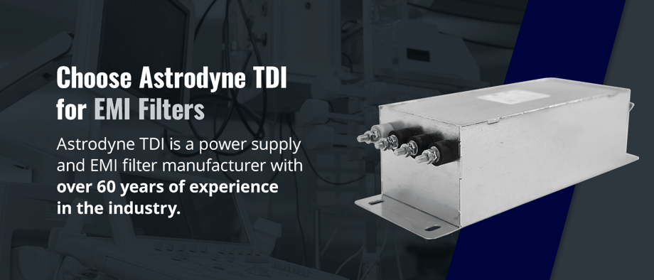
Choose Astrodyne TDI for EMI Filters
EMI solutions, including semiconductor EMI filters, are a necessity in the semiconductor manufacturing industry. Unfortunately, various technical requirements can prevent you from finding the perfect semiconductor EMI filters in off-the-shelf solutions. If you're looking for a manufacturer that can match you with quality solutions, Astrodyne TDI is here to help.
Astrodyne TDI is a power supply and EMI filter manufacturer with over 60 years of experience in the industry. We produce EMI, EMC and RF filters for a variety of industries, from the medical and industrial industries to semiconductor manufacturing facilities. On top of our quality off-the-shelf solutions, we have advanced tools and technology to design and modify power supplies and EMI filters, so we can build a custom solution that meets your unique requirements.
Learn more about our EMI filter solutions and contact us today.