RESOURCES
EXECUTIVE SUMMARY
A key change instituted in the 4th edition of the medical EMC standard 60601-1-2, 4th ed, is to test practically all medical devices up to ESD level 4, 15KV air discharge, and 8KV direct discharge. Whereas in the 3rd ed only life support and critical medical devices required this relatively high ESD test voltage. At the 15KV level, it is imperative to use the proper ESD test protocol to obtain accurate test results, and not induce power supply damage by capacitance charge ratcheting.
ESD CHARGE RATCHETING ISSUE
The typical problem associated with failure to properly remove the charge and voltage from the product under test during ESD testing is voltage ratcheting upwards, with each subsequent ESD pulse event. The voltage steps which occur, are computable, and using special test equipment and procedures, this voltage stepping action has been confirmed. In the diagram below, a typical power supply isolation barrier capacitance of 1085pF is examined, thru simple mathematical means, to show the charge voltage stepping action for 16 sequentially applied +15KV ESD pulses.
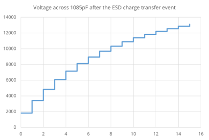
If a 230VAC input rated Class II power supply is to meet the touch current 100uA requirement at the output leads, then the capacitance across the isolation barrier must be somewhere around 1000pF. For this specific analyzed power supply in this example, a network of several capacitance values achieves a total Class II isolation barrier capacitance of nominal 1085pF.
Several circuit components cross the isolation barrier in the power supply. Typically, these will be:
- Transformer
- Optocoupler
- EMI filter capacitors are often referred to as “bridging capacitors”
When two Y1 bridging capacitors are used in series across the isolation barrier, which is typical in a medical power supply, the resulting pair of caps may withstand 14KV peak blocking voltage. However, the optocoupler and the transformer will typically not withstand that level, usually, 10KV is the maximum blocking voltage these components can withstand before the isolation will breach/fail. In the case of the optocoupler, this will typically destroy the optocoupler if the breach is internal to the device, in the case of the transformer, the breach will typically not damage the transformer, but semiconductor components on either side of the transformer breach location may fail due to excessive voltage stress.
Therefore, it is not good to allow subsequent ESD pulse events to ratchet up the voltage across the isolation barrier to the point of component failure. The 61000-4-2 standard warns against this in section 7.2.4.1 “Ungrounded Equipment”. It states on pages 18 and 19 of the 2008 version:

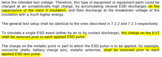
The above statement clarifies the problem, yet does not clarify the method to remove the unrealistically high accumulated charge voltage resulting from multiple sequential ESD pulse events. And the lack of clarity on the method to remove the accumulated charge is the fundamental reason typical power supplies will fail the 15KV air discharge ESD test.
Perhaps some confusion in the wording of the standard maybe is created from the following statement which directly follows the above section: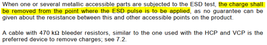
In the above section, it’s clear the ESD applied point is metallic, which makes sense since ESD does not discharge directly to plastic. However, the standard method to apply the air discharge ESD pulse to the EUT will look for voids or cracks in a plastic housing which can arc from the ball tip of the ESD gun. After the discharge is applied, simply swiping the plastic with the carbon fiber brush will not remove the charge. To remove the charge the metallic point of ESD injection must be directly contacted for correct charge removal.
NEUTRALIZING ELECTROSTATIC CHARGE
Removal of the charge at the exact point of the ESD charge application may need to be done with a thin metal contact that can reach between the plastic housing, connected to the above-mentioned two 470K ohm resistors. Metallic contact only needs to be maintained for a few milliseconds to dump the typical accumulated charge.
Another point of charge removal is the output of the power supply. Since the charge is being stored across the “capacitance of the Class II Insulation”, which is located within the power supply. The power supply output, typically the negative output terminal, is an ideal place to remove the charge. This point in most medical devices powered by an external power supply (AKA power adapter), can be reached by disconnecting the DC output connector from the medical device. Another more convenient way is to solder a short wire to the negative output terminal of the power supply and apply the accumulated charge removal at this now accessible circuit point.
Besides the removal of accumulated charge using a direct path thru a pair of 470K ohms resistor, the ESD standard mentioned the “self-discharge” method, the text shown below: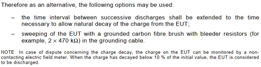
Unfortunately, this method may not be practical from a time perspective. Our evaluation showed only a 2% voltage reduction at 2 minutes from an accumulated charge voltage on 1000 to 2000pF capacitance. This works out to several Petra-ohms of resistance, and the time required to self-discharge the capacitance across the Class II isolation barrier is extremely long. There may be types of Class II isolation barriers that have a 1000x lower resistance, but at the present, these have been identified.
Should the concept of removing the charge from the EUT ESD injection point between plastic seams in the medical device, at the Class II isolation barrier, cause a bit of a queasy feeling due to confusion in the standard, there is another method which I recently developed, which can alleviate the need for different ESD injection points and charge removal points on the EUT, which I refer to as the alternating polarity ESD injection method.
This new method is simply applying +15KV, then changing to -15KV, repeating this sequence 10 times. This is in contrast to the normal method of applying ten +15KV ESD pulses sequentially, then changing to -15KV pulses, applied ten times. Below are the expected voltage levels across the Class II isolation barrier: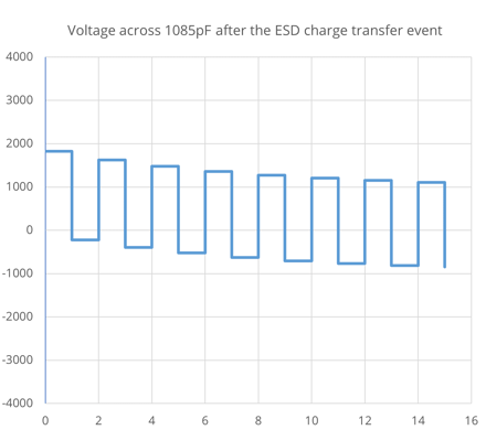
From the above, it is noted that the first step produces essentially a +2000V residual voltage on the isolation barrier after the first positive ESD pulse. The second negative ESD pulse brings the accumulated voltage to slightly below zero volts. Continuation of the pattern results in the eventual positive and negative plateaus approximating +/-1000V.
The above shows 16 ESD pulses, but to meet the necessary minimum requirement in the ESD standard, a total of 20 pulses (2x10) would be required. Additionally, it would be strongly recommended to discharge any accumulated residual charge voltage from the power supply between voltage level shifts, just to keep from introducing drifting of the charge voltage on the Class II isolation barrier when going they the multiple level shifts. The most important point when to dump any residual charge voltage at the Class II isolation barrier would be between the +/-8KV air and +/-15KV air levels transition.
PRESCANNING AT 20 PULSES PER SECOND, BE CAUTIOUS
Identification of ESD sensitive points on keyboards and housings will often involve setting the ESD gun at a rapid repetition rate, this concept is described on the top of page 26 in the 2008 version of the standard:

The concern with overstressing the product is of course a major factor. Without a return path for the ESD charge to be dissipated within a short period (milliseconds), the charge voltage will quickly ratchet up to the destruction point of the Class II isolation barrier components, when the ESD gun is set at +/-15KV. If the exploratory approach is to be used, then it becomes necessary to ground the negative output of Class II power supply back to earth thru the pair of 470K-ohm resistors. Note, with up to 5000pF of capacitance the discharge time for one time constant is:
5000pF x 940K-ohm = 4.7 milli-seconds
And 4.7 milli-seconds is far below the 50 millisecond period when the ESD gun repetition rate is 20 pulses per second.
CLASS II POWER SUPPLIES WITH FUNCTIONAL EARTH:
3 TERMINALS AT AC INPUT
When a power supply has a 3 conductor AC input connector, this does not make it a Class I power supply. The Class I designation indicates either:
- The output of the power supply is earthed, or
- The power supply is in a metal housing, and the housing is earthed. In this case, the output may be floating or earthed.
In the typical situation of a plastic housed power supply, when a 3 conductor AC input configuration with one lead earthed is used, the output may either be floating or earthed. If earthed, then the configuration is properly called a “Class I” configuration. If the output is floating, then the configuration is properly called a “Class II with Functional Earth” configuration.
The importance of this is obvious, with the output floating, the isolation barrier will develop a charge voltage ratcheting when exposed to ESD pulses. However, if the output was earthed, it could not. Therefore, whenever a 3 conductor AC main connection with the earth is encountered in the ESD lab, it is important to determine if the output is floating or not. Should the output be floating, then it is a Class II power supply, and must be treated per the requirements of the ESD standard for section 7.2.4, Ungrounded Equipment, in the same way, that an ordinary Class I power supply would be.
MODIFICATION TO THE EMC TEST PLAN:
As brought to my attention recently, for an orderly EMC test process on any product to occur, a reasonably comprehensive test program from the equipment manufacturer should exist. When problems crop up during ESD testing at 15KV such as described above, and the test protocol is modified to prevent charge voltage ratcheting on the isolation barrier components, it is good practice to note whatever modifications to the standard protocol were used during the testing. In the recent scenario, a simple 2 or 3 sentences describing the alternate polarity application of the ESD pulses would suffice, this need would be added to the EMC test plan.
Similarly, if a wire is brought out from the negative lead of the DC output connector of the power supply, and a pair of 470K-ohm resistors are series hooked up to the ground from this point to prevent charge voltage ratcheting. Simply add this description to the test plan.
FOR REFERENCE:
A schematic model of the ESD charge transfer event, and a simplified model as well, are shown below. Note, only the key elements as it applies to typical product scenarios, are shown.
The voltage which results in the Class II isolation barrier is shown as the variable Vx, for the first ESD discharge pulse. For subsequent pulses, the incremental increase in voltage is slightly less after each discharge, since the voltage difference driving variable, is no longer 15KV – zero volts.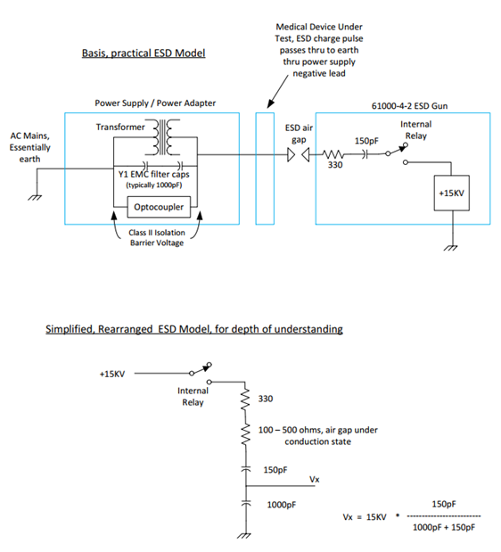
ABOUT THE AUTHOR
 David Love
Principal Engineer
David Love is a third-generation power supply electrical engineer, presently specializing in DC power supplies from 1W to 1000W output power level. He has spent 30 years working with compliance engineers worldwide in safety and EMC labs. For 10 years he managed a Manufacturers Data Program test lab for medical and ITE products while working at Jerome Industries which was acquired by Astrodyne in 2009.