RESOURCES
Of all the likely scenarios encountered by a regulated power supply, running in the steady-state condition with a fixed resistance is but one situation. An application will often involve conditioning power for loads that are time-variant and nonlinear: Those that pulse the load current are of interest here.
The pulse repetition frequency and duty cycle of the load are the defining system parameters used to assess what the power supply needs to deliver. A load surge sees elevated currents in the load that change slowly with time, the other extreme being the very rapid transient events characterized by short, sharp spikes in load current.
A surge event might occur for instance as a centrifuge “spins up”; As it begins to rotate up to the very high speeds that are called for, the torque applied to it must be maximized for several tens of seconds. The motor is fed with a higher current compared to its steady-state power demand. Once running at full speed, the centrifuge’s current draw drops to a level sufficient to overcome friction and drag. We distinguish between the 2 power draw states as being either “peak” (heavy load) or “base” (lightly loaded) mode.
An SMPS (switched-mode power supply) should be designed in such a way that this kind of operation is anticipated during the concept stage. Considerations involve the technologies (covering composition, physical and electrical characteristics) of the switches, thermal interfaces, design of heatsinks, and other external cooling elements - be it forced-air, vapor phase, or liquid cooling - to cope with heat flashes within the switches.
Contrast this with the transient nature of loads encountered in a radar transmitter. To clearly define a target return, the system broadcasts very short, sharply defined pulses. Power solutions that support radar are designed to minimize the system’s susceptibility to the harmonic-rich spectrum of output power. This is done to ensure the control signal integrity of the power supply.
The intent is to show a “first cut” method of analysis that will help determine how transient pulsing loads affect a power supply.
The Right Power Solution for a Pulsed Load
“Is there a simple model of a regulator which can be used to gauge its reaction to transient pulsed loads?” is a question that comes up quite often. Another associated question is “how do I select a workable power solution for such loads?”.
The proposed model does not account for feedback. If the reader wants to explore internal feedback control techniques used in Astrodyne TDI’s product, they would do well to refer to the application note “Constant Voltage, Constant Current and Constant Power” that has been recently published on the Astrodyne TDI web portal, by design engineer Stephen Innis. It features an informative, practical view of the nature of SMPS regulator control afforded within Astrodyne TDI’s switched-mode power supplies. Learnings from this article could be used as the basis to develop more detailed models that account for the reaction of the regulator to sudden load changes.
Power Stage LTSpice™ Modeling
Model development
The LTSpice™ model is assessed initially using a simple DC transfer function analysis, followed by a suitably arranged transient analysis.
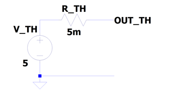
Figure 1 – Thevenin voltage source equivalent circuit for example 5V regulator output port
A Thevenin equivalent voltage source is shown in figure 1. In a power setting, this serves a load connected across its port with the voltage held as a straight line - with a small negative gradient - between the minimum and maximum current levels. Within this range of output currents, the voltage regulator can hold a voltage setpoint that changes within a very narrow margin, typically stated as a percentage deviation. For example, if the task was to model a 5V regulator’s output port, a load regulation (error) of no more than +/- 1% equates to +/- 50mV change across a load as it draws a current. The current draw may vary from as little as 10% of full load to the maximum, or 100% of the rated, or nominal load. If the rated load is 10A then the compliance of the regulator is 1 to 10A.
The drawback with this model is that it does not exhibit the sort of current limiting that would be expected in a real-world voltage regulator. This type of limiting action is different from the situation where protection against inadvertent short-circuiting is mandated. Going back to the 5V regulator example, we might peg the current limit plateau to 10A in our example. At the levels slightly higher than the nominal, expect to see a slight reduction of output voltage, rather than a complete shutdown of the regulator.
Final Model
A pulsed load would move the operating point of the regulator’s output power port between low-current (base) maximum-current (peak) levels. A model that mimics brick-wall current-limiting behavior is shown in figure 2.
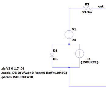
Figure 2 – Current-limited constant voltage source
Under the conditions depicted in figure 2 (open circuit load) current I1 flows through diode D1. This diode is ideal – it exhibits no forward voltage when forward biased. The voltage across the model’s single port in this condition is V1. The ideal diode prevents the current source from developing voltage.
With a load in place, the difference between the load current leaving the {out} node and the constant current source I1 is the current in diode D1. When the load current reaches 10A, D1 stops carrying current; the current in V1 is the same as I1. A voltage difference now develops across I1 as D1 is now reverse biased. The reverse bias current in D1 is negligible.
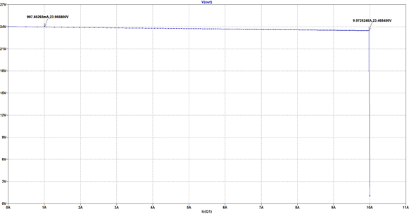
Figure 3 – Current and Voltage Operating Characteristic of the current limited voltage source
The static characteristic for the current limited voltage source is plotted in figure 3. Notice the negative gradient on the topside of the characteristic, continuing up to the current limit threshold. This gradient is attributed to small signal resistor R3. The model is now ready to be used to mimic the behavior of the power supply to first order.
Understanding Load Transient Response
A rule of thumb in switching power supply feedback loop design is that loop bandwidth should not exceed between 1/10th to 1/6th of the switching frequency of the SMPS. The control loop is slow to resolve a transient condition brought on by a pulse edge if its time constants are large in comparison with the rise- or fall-time of current in the load. The physical structure of the power bus with series inductance being the dominant factor, and frequency-dependent ESR and ESL (estimated series resistance and inductance respectively) of decoupling capacitors determine the nature and size of excursions of voltage from its setpoint with each successive onset and removal of maximum load.
Simulating a single pulse is sufficient for testing a prospective solution. It will indicate how well a selected decoupling capacitor - connected across the regulator’s output port - can transfer the charge it stores into the load. It will also show how quickly it is able to replenish itself after the single pulse has been applied and removed. The capacitor is fully charged prior to the load pulse. We observe that the regulator output voltage dips and then rebounds soon after the load is turned off, thanks to the regulator returning to its voltage setpoint, recharging the decoupling capacitor during the pause before the next load pulse arrives. In an ideal system, the voltage dip and the recharge times are kept within limits commensurate with the pulse repetition frequency.
A simulation can be set up that reflects practical limitations imposed on the regulator and output decoupling capacitor combination. It is the intent here that the reader will be able to work within the limitations of the system: the power output of the regulator, size and technology of the decoupling capacitor, and the load pulse duty cycle and repetition frequency. This will minimize the effort to achieve a well-founded pulsed load power supply.
Pulsed Power Case Study
Thermal print heads use large, pulsed currents to affect the print medium. The engineer responsible for powering the accessories in a weigh scale got in touch to see if a specific regulator we had in the product portfolio could be used to power not just the printer, but the entire system. The customer’s view was that a large-cap might be used to help smooth out the demand of the print head.
Some calculations were made to show that this initial concept would not work. However, these in addition to the simulations provided could be used by the customer to explore alternative setups.
Astrodyne TDI applications engineers examined oscillograms obtained with a laboratory power supply. These ‘scope shots pertain to a particular part of the printing operation during which a heavy black print is made – the printhead system draws the largest amount of power in this phase of operation, forming a “worst-case” scenario. If the selected power supply meets this demand, the system would be expected to work well under normal operational conditions. The worst-case load format comprises a base current of about 2.5A DC. Superimposed on this are 19 consecutive current pulses that peak at 12A with a 500 usec duration and 50% duty cycle.
Power Estimate
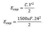
The average power, Pav required by the print head over the duration of 19 msec (covering 19 sequential pulses with 50% duty cycle) is given by
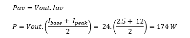
This is about 2.5 times the nominal rating of the proposed regulator. The energy required for sustaining a single pulse along with the baseload would be 174 x 1 msec = 0.17 Joules.
Comparing Calculation and Simulator Outcomes
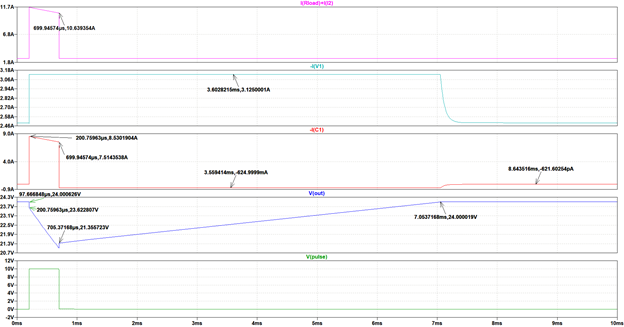
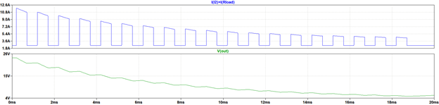
Figure 4 shows the originally proposed circuit configuration simulated in LTSpice™ with outcomes in figure 5. Several measurements appear on the plots to help divine what processes are occurring in the circuit. The base and pulse elements of the load current have been added together in the top-most plot. The drawdown of charge is manifest in the current delivered by the capacitor, moving from 8.5A to 7.5A. After the load pulse has been serviced, current from the regulator is switched to the capacitor, allowing it to recover all the charge it lost to the pulsed load, a process which takes about 6.4 msec. The simulated capacitor current is by convention negative when it is being impressed on the capacitor’s positive electrode. It is held constant at 625 mA. Once the capacitor has recovered, the current from the regulator drops from the nominal level of 3.125A to 2.5A to service the baseload alone. The information revealed in the simulation run compares well with figures based on theory which is provided in the appendix.
ESR for the decoupling element C1 is a typical value for an electrolytic capacitor of its size. The effect of the capacitor ESR is seen in its voltage every time a sharp current pulse appears in it. With the onset of load, for example, we can see that there is an instantaneous change in the output voltage of (24.00 – 23.62) = 380 mV. This is caused by the voltage drop across the capacitor which exhibits an impedance commensurate with only its ESR of 44 mW. The current at the rising load pulse edge is estimated to be 380mV/44mW = 8.65A which is close in value to the peak current in the capacitor C1 of 8.53A.
In the simulator outcome of figure 5, observe that the capacitor recovers its charge in time for another power pulse after 6.4 msec.
The minimum sustainable cycle time is the sum of pulse ON time and recovery time i.e. [0.5 + 6.4] msec = 6.9 msec. This corresponds to a maximum allowable pulse repetition frequency of [1/0.0069] = 144 Hz. The pulse repetition rate that this application can support is 7 times lower than the required 1 kHz. Note that the amount of energy stored in the charged capacitor is inversely proportional to the amount that voltage “dips” during the load pulse. There is clearly a compromise between the permitted dip in voltage which dictates the size of the capacitor and the pulse repetition frequency for a given regulator power rating.
The load voltage dip that can be tolerated during pulsing must be specified. With this number to hand, you can determine the nominal power rating of the regulator and the size of the capacitor.
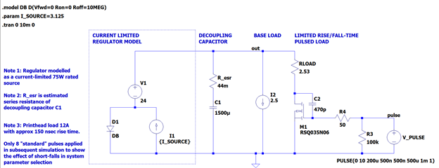
Figure 4 LTSPICE™ schematic for a single 500usec duration load pulse
Assessing Original Configuration
Examining figure 6, currents during pulse delivery sum in this way
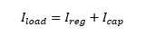
From which 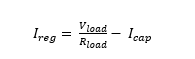 equation [1]
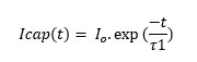
With a load being pulsed ON, the capacitor current discharges exponentially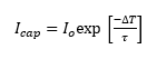 equation [2]
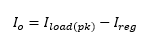
Noting that { Io } is the instantaneous peak current that the capacitor provides – this being the difference between the peak load current and the regulator’s nominal current
As the regulator supplies fixed current { I_reg }, we see that it is the capacitor’s variable current supply that dictates the size of output voltage dip on examination of equation [1]
 equation [3]
With DT = 500 usec, Io = 8.875A, t = (RPulsed_load .C) = 3.1 msec, with C= 1500uF and RPulsed_load = RPULSE + RSW = 2.05W - we find the change in load voltage brought about by a load pulse - using equation [3]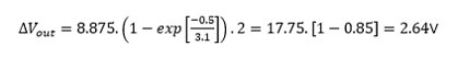
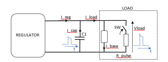
Figure 6 – currents and voltage designations during load pulse delivery
Building on the Basic Need
If the converter’s nominal power is less than the estimate made to sustain the load, we can expect to see the peak output voltage sagging with each successive pulse in the full pulse comb that the system must ultimately sustain.
If the voltage dip with the onset of the load is to be no more than 500mV and converter power set to 174W, we can determine the required value for the decoupling capacitor.
Calculate the peak capacitor current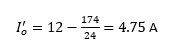
We now find the required time constant associated with the load and the decoupling capacitor. Knowing what the load is, we find the sustaining value for the decoupling cap:
Rearranging equation [3] and applying values, we find that
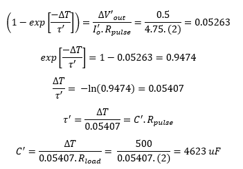
Checking this, we have time constant C’ x R = 9.246 msec, from which we can back-calculate the voltage dip i.e the change in voltage that occurs during load pulsing:
Note that the resistance of the MOSFET switch has been neglected in this instance, resulting in a slightly larger capacitance figure.
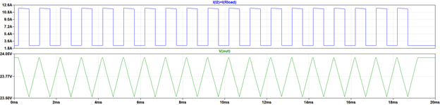
Heavy Load Case Outcomes
The simulation outcomes for the heavy print case are shown in figures 7(a) and 7(b) for the original and the new system respectively. Figure 7(a) shows pulses in the original circuit successively reducing in amplitude, with output voltage dropping away significantly – implying a disappearing print signature. Contrasting with this, the pulse cycles in the reconfigured circuit are identical and correctly formed. The voltage dips are 500 mV; there is no “sag” in the overall shape of the voltage waveform during the pulse stream – the system could run in this way indefinitely. The decoupling capacitor recovers fully between successive load pulses; the output voltage contains no artifacts from the previous pulse event.
(a)
(b)
The simulator model comes into its own: You can experiment with increasing the power beyond the minimum needed, seeing the effect on the depth of the voltage dips and the spacings of the dip and rise combinations, implying that the pulse repetition frequency can now be increased – you’re invited to try it out and see. You can figure out the effects of differing power and capacitor combinations with the calculations. With more power, expect the voltage dips to start to become very small even with very high pulse repetition frequencies in play. You can include bus inductance as well: The choices you can explore with the approach outlined here should hopefully be informative.
Conclusion
This article addresses the subject of regulator and decoupling capacitor sizing for pulsed loads of a transient nature. A first-order model has been described and deployed. Readers can make refinements that can account for the speed and precision of the regulator feedback loop(s). Although mentioned, no account has been made of bus inductance, which can make significant contributions to voltage changes on the power bus. There are also perplexing situations involving resonances within capacitor banks containing low ESR components which remain unaddressed here.
APPENDIX – Verifying the Large-Signal Model
During each 1 msec cycle in the printer head case study, the pulsed load draws current from the large-cap and the regulator it decouples in 500usec, and when the pulse is absent, the regulator is expected to recharge the cap’s voltage back to 24V in 500usec whilst supplying the load.
If we take one ideal pulse only, the total energy in Joules absorbed in the load is given by

The decoupling cap initially has stored energy commensurate with being charged to 24V DC
Which is 0.432 Joule: about 3 times the energy required to sustain a pulse.
The capacitor, when connected to the load, discharges. The current is determined using the well-known expression
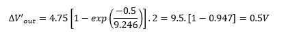
In the formula, is the RC time constant of combined load along with the MOSFET switch - which has a small resistance of about 50 mW. In this case, the exact time constant works out to be 3.075 msec (the product of 2.05W and 1500 uF).
After 500 usec, the capacitor current drops from 8.875A (the difference between the load demand at 24V and the constant current of the regulator) to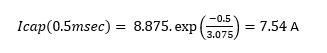
The voltage at the load after 500 usec is simply loaded resistance multiplied by the combined cap and the regulator currents it sinks

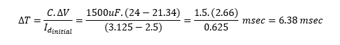
Once the load pulse has come and gone, the capacitor begins charging: The paralleled capacitor and baseload have an initial voltage of 21.34V. The initial charge current available to the capacitor is the nominal current of the regulator minus the load’s base current. We can find approximately how long it will take before the capacitor’s lost charge is fully restored. To find this time, we determine the slope of voltage rise at this point and then find the approximate charge time DT by accounting for the difference between the voltage of the capacitor initially and the final value, so the current available for charging is
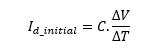
Where Id_initial is the difference between the nominal regulator and the baseload currents and DV is the difference in voltage to be made up
From this equation, we find